陶瓷天线
 文件编号: FH-TC-007
陶瓷天线简介
拟制: 审核: 日期:
|
陶瓷天线简介瓷天线简介 陶瓷天线简介 |
陶瓷天线
陶瓷天线是一种用于通信、导航、雷达等领域的天线器件。它具有体积小、重量轻、频宽宽、耐温性好、抗干扰能力强等特点,被广泛应用于移动通信、卫星导航、飞行器等领域。下文以一款蓝牙天线为例,介绍其制造工艺流程。
1.陶瓷材料制备
陶瓷材料的选择直接影响天线的性能指标。一般选用介电常数大,损耗小的瓷质材料。陶瓷材料的制备方式有多种,常见的有注浆成型法和压延成型法。本案例采用注浆成型法,即将陶瓷粉末与有机溶剂按一定比例混合后,注入模具中进行成型,再通过干燥、清洗等工艺步骤得到成品。
2.金属化处理
陶瓷材料具有较好的介电性能,但其导电性能不足。因此,需要通过金属化处理提高导电性能。金属化处理一般采用化学镀银、真空蒸镀、电化学镀等方式。本案例采用化学镀银法。具体工艺流程如下:
(1) 清洗:将已经成型的陶瓷天线进行水洗、超声波清洗等工艺处理,出去表面杂质和油脂。
(2)酸洗:将清洗好的陶瓷天线放入硝酸中进行酸洗,去除陶瓷表面的氧化层,并为后续步骤提供光洁表面
(3)化学镀银:将经酸洗处理的陶瓷天线浸入含有AgN03的银水中,经过还原反应后在陶瓷表面渡上一层粒子从而实现金属化处理。
3.组装配件
将金属化处理好的陶瓷天线,同其他金属组件(如中性点、馈线)进行组装。组装方式有焊接、粘接、压装等多种方式,本案例采用压装方式。将组件通过机械压力压合,形成一个整体,达到确保天线性能稳定的目的
4.组装完成后,需要对天线进行调试测试。测试内容主要包括天线增益、轴比、驻波比等多项指标。
下面为一例陶瓷天线各项测试数据示例:
|
Engineering Specification
1 .Product Number |
||||||||||||||||
|
FH |
3216 2 |
Q2 ;3 |
3
4 |
2P52
5: |
||||||||||||
|
|
||||||||||||||||
|
|
深圳市福汇科技有限公司 SHEN ZHEN FUHUI TECHNOLOYCO.,LTD. |
|||||||||||||||
|
Prepared by:JIEXI Designed by:Jason Checked by:Jason Approved by: MR.FANG |
||||||||||||||||
|
TITLE :3.2×1.6x0.5(mm)WiFi/Bluetooth Ceramic Chip Antenna (YF3216H2)Engineering Specification |
DOCUMENT NO. |
FH3216Q23P52 |
REV. |
|||||||||||||
|
B |
||||||||||||||||
|
PAGE 1 OF 13 |
||||||||||||||||

|
2.Features *Stable and reliable in performances *Low temperature coefficient of frequency *Low profile,compact size *RoHS compliance *SMT processes compatible 3.Applications *Bluetooth earphone systems *Hand-held devices when WiFi /Bluetooth functions are needed,e.g.,Smart phone. *IEEE802.11 b/g/n *ZigBee *Wireless PCMCIA cards or USB dongle
4.Description Yingfeng chip antenna series are specially designed for WiFi/Bluetooth applications.Based on yingfeng proprietary design and processes,this chip antenna has excellent stability and sensitivity to consistently provide high signal reception efficiency. 5.Electrical Specifications (80x40 mm²ground plane)
|
||||||||||||||||||||||||||||||||||||
|
|
深圳市福汇科技有限公司 SHEN ZHEN FUHUI TECHNOLOYCO.,LTD. |
|||||||||||||||||||||||||||||||||||
|
Prepared by:JIEXI Designed by:Jason Checked by:Jason Approved by: MR.FANG |
||||||||||||||||||||||||||||||||||||
|
TITLE :3.2×1.6x0.5(mm)WiFi/Bluetooth Ceramic Chip Antenna (YF3216H2)Engineering Specification |
DOCUMENT NO. |
FH3216Q23P52 |
REV. |
|||||||||||||||||||||||||||||||||
|
B |
||||||||||||||||||||||||||||||||||||
|
PAGE 2 OF 13 |
||||||||||||||||||||||||||||||||||||

|
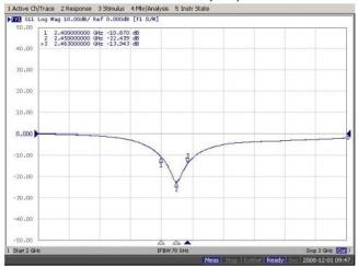
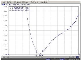
5-2.Return Loss &VSWR
Return Loss (Si) VSWR(S11) |
|||||||||||||||||||
|
|
|
||||||||||||||||||
|
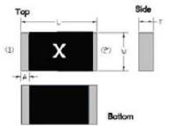
6 .Antenna Dimensions &Test Board (unit:mm) a.Antenna Dimensions
Dimension and Terminal Confiquration |
|||||||||||||||||||
|
|
|
|
|||||||||||||||||
|
|
深圳市福汇科技有限公司 SHEN ZHEN FUHUI TECHNOLOYCO.,LTD. |
||||||||||||||||||
|
Prepared by:JIEXI Designed by:Jason Checked by:Jason Approved by: MR.FANG |
|||||||||||||||||||
|
TITLE :3.2×1.6x0.5(mm)WiFi/Bluetooth Ceramic Chip Antenna (YF3216H2)Engineering Specification |
DOCUMENT NO. |
FH3216Q23P52 |
REV. |
||||||||||||||||
|
B |
|||||||||||||||||||
|
PAGE 3 OF 13 |
|||||||||||||||||||

|
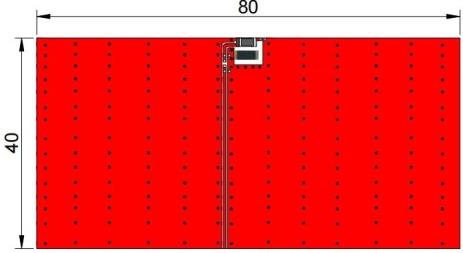
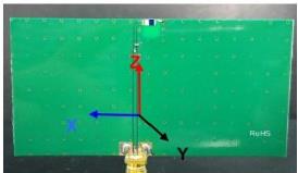
b.Test Board with Antenna
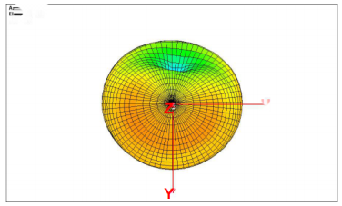
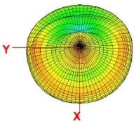
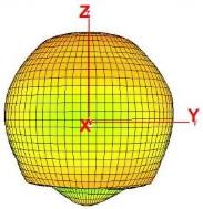
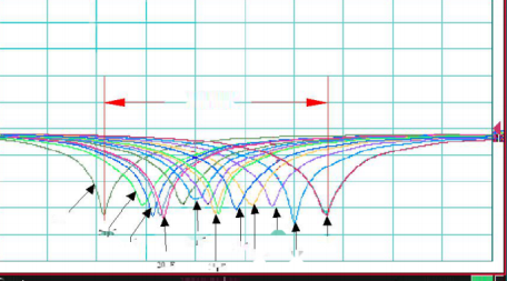
7.Radiation Pattern (80x40 mm²ground plane 7-1.3D Gain Pattern @2442 MHz
Roll-0.0
X |
||||||
|
|
深 圳 市 福 汇 科 技 有 限 公 司 SHEN ZHEN FUHUITECHNOLOYCO.,LTD. |
|||||
|
Prepared by:JIEXI Designed by:Jason Checked by:Jason Approved by:MR.FANG |
||||||
|
TITLE:3.2x1.6x 0.5(mm)WiFi/Bluetooth Ceramic Chip Antenna (YF3216H2)Engineering Specification |
DOCUMENT NO. |
FH3216Q23P52 |
REV |
|||
|
B |
||||||
|
PAGE 4 OF 13 |
||||||

|
|
|||||||||||||||||||||||||||||||||||||||||||||||||||||
|
|
|
||||||||||||||||||||||||||||||||||||||||||||||||||||
|
7-2.3D Efficiency Table
|
|||||||||||||||||||||||||||||||||||||||||||||||||||||
|
|
深圳市福汇科技有限公司 SHEN ZHEN FUHUI TECHNOLOYCO.,LTD. |
||||||||||||||||||||||||||||||||||||||||||||||||||||
|
Prepared by:JIEXI Designed by:Jason Checked by:Jason Approved by: MR.FANG |
|||||||||||||||||||||||||||||||||||||||||||||||||||||
|
TITLE :3.2×1.6x0.5(mm)WiFi/Bluetooth Ceramic Chip Antenna (YF3216H2)Engineering Specification |
DOCUMENT NO. |
FH3216Q23P52 |
REV. |
||||||||||||||||||||||||||||||||||||||||||||||||||
|
B |
|||||||||||||||||||||||||||||||||||||||||||||||||||||
|
PAGE 5 OF 13 |
|||||||||||||||||||||||||||||||||||||||||||||||||||||

|
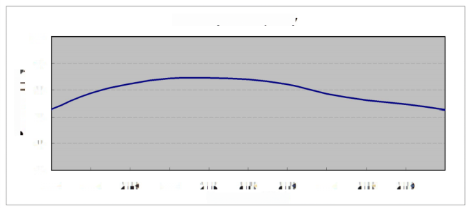
7-3.3D Efficiency vs.Frequency |
|||||||
|
100 |
|||||||
|
Efficiency(%) |
90
80
70
60
50 2400 2410 |
2420 2430 |
2442 2450 2460 Frequency(MHz) |
2470 2480 2490 2500 |
|||
|
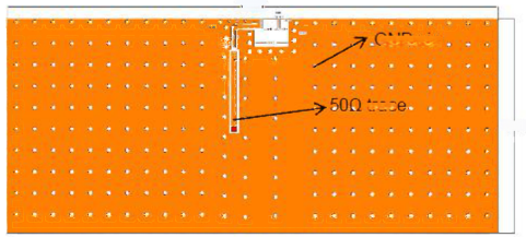
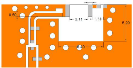
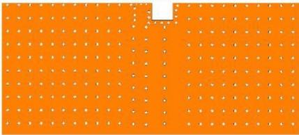
8.Layout Guide a.Solder Land Pattern: Land pattern for soldering (gray marking areas)is as shown below.Depending on Customer's requirement,matching circuit as shown below is also recommended
SNDVIa
名 [ 40.00
Top view |
|||||||
|
|
深 圳 市 福 汇 科 技 有 限 公 司 SHEN ZHEN FUHUITECHNOLOYCO.,LTD. |
||||||
|
Prepared by:JIEXI Designed by:Jason Checked by:Jason Approved by:MR.FANG |
|||||||
|
TITLE:3.2x1.6x 0.5(mm)WiFi/Bluetooth Ceramic Chip Antenna (YF3216H2)Engineering Specification |
DOCUMENT NO |
FH3216Q23P52 |
REV |
||||
|
B |
|||||||
|
PAGE 6 OF 13 |
|||||||

|
Unit:mm
|
|||||
|
2.60 1.60 |
5 |
||||
|
Detail view
Bottom view |
|||||
|
|
深 圳 市 福 汇 科 技 有 限 公 司 SHEN ZHEN FUHUITECHNOLOYCO.,LTD. |
||||
|
Prepared by:JIEXI Designed by:Jason Checked by:Jason Approved by:MR.FANG |
|||||
|
TITLE:3.2x1.6x 0.5(mm)WiFi/Bluetooth Ceramic Chip Antenna (YF3216H2)Engineering Specification |
DOCUMENT NO. |
FH3216Q23P52 |
REV |
||
|
B |
|||||
|
PAGE 7 OF 13 |
|||||

|
9.Frequency tuning
b.Matching circuit:(Center frequency is about 2442 MHz @80x40 mm²ground plane) |
||||||||||||||||||||||||||||
|
|
|
|||||||||||||||||||||||||||
|
*Typical reference values which may need to be changed when circuit boards or part vendors are different. |
||||||||||||||||||||||||||||
|
|
深圳市福汇科技有限公司 SHEN ZHEN FUHUI TECHNOLOYCO.,LTD. |
|||||||||||||||||||||||||||
|
Prepared by:JIEXI Designed by:Jason Checked by:Jason Approved by: MR.FANG
|
||||||||||||||||||||||||||||
|
PAGE 8 |
OF |
13 |
||||||||||||||||||||||||||
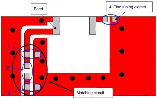

c.Fine tuning
Center 2.45 |
element vs.Center frequency |
|||||||
|
|
||||||||
|
02
GH |
S0pE 39pF |
15pF 22pF |
6pF 8pF 7pF 5pF 10pF |
4pF
Span 500 M-e c? |
||||
|
IFEW 70 kHe |
||||||||
|
|
深圳市福汇科技有限公司 SHEN ZHEN FUHUITECHNOLOYCO.,LTD. |
|||||||
|
Prepared by:JIEXI Designed by:Jason Checked by:Jason Approved by:MR.FANG |
||||||||
|
TITLE:3.2x1.6x 0.5(mm)WiFi/Bluetooth Ceramic Chip Antenna (YF3216H2)Engineering Specification |
DOCUMENT NO. |
FH3216Q23P52 |
REV |
|||||
|
B |
||||||||
|
PAGE 9 OF 13 |
||||||||

|
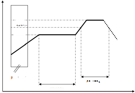
10.Soldering Conditions a.Typical Soldering Profile for Lead-free Process |
||||||
|
11.Packing |
150-200°
Pre-heati 60-150s 60-180s Time |
|||||
|
(1)Quantity/Reel:6000 pcs/Reel |
||||||
|
|
深圳市福汇科技有限公司 SHEN ZHEN FUHUITECHNOLOYCO.,LTD. |
|||||
|
Prepared by:JIEXI Designed by:Jason Checked by:Jason Approved by:MR.FANG |
||||||
|
TITLE:3.2x1.6x 0.5(mm)WiFi/Bluetooth Ceramic Chip Antenna (YF3216H2)Engineering Specification |
DOCUMENT NO |
FH3216Q23P52 |
REV |
|||
|
B |
||||||
|
PAGE 10 OF 13 |
||||||

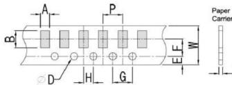
 Reel Specification
Reel and Taping Specification
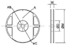
|
TYPE |
SIZE |
A |
φB |
φC |
φD |
W |
φM |
|
|
3216 |
7” |
5K/Reel |
2.0±0.5 |
13.5±1.0 |
21±1.0 |
60±1.0 |
11.5±2.0 |
178±2.0 |
Tapping Specification
T
|
Packaging |
Type |
A |
B |
W |
E |
F |
G |
H |
T |
φD |
P |
|
Paper Type |
3216 |
1.90±0.20 |
3.50±0.20 |
8.0±0.20 |
1.75±0.10 |
3.5±0.05 |
4.0±0.10 |
2.0±0.05 |
0.75±0.10 |
+0.10 1.50 -0 |
4.0±0.1 |

Prepared by:JIEXI
深圳市福汇科技有限公司
SHENZHEN FUHUI TECHNOLOYCO.,LTD.
Designed by:Jason Checked by:Jason Approved by: MR.FANG
TITLE:
3.2×1.6x 0.5(mm)WiFVBluetooth Ceramic Chip Antenna (YF3216H2)Engineering Specification
DOCUMENT
NO.
FH3216Q23P52
PAGE 11
OF
REV.
B
13
|
|
||||||||||||||||
|
|
深圳市福汇科技有限公司 SHEN ZHEN FUHUI TECHNOLOYCO.,LTD. |
|||||||||||||||
|
Prepared by:JIEXI Designed by:Jason Checked by:Jason Approved by: MR.FANG |
||||||||||||||||
|
TITLE: 3.2×1.6x0.5(mm)WiFi/Bluetooth Ceramic Chip Antenna (YF3216H2)Engineering Specification |
DOCUMENT NO. |
FH3216Q23P52 |
REV. |
|||||||||||||
|
B |
||||||||||||||||
|
PAGE 12 OF 13 |
||||||||||||||||

|
Reliability Table
|
||||||||||||||||||||||||||||||||||||
|
|
深圳市福汇科技有限公司 SHEN ZHEN FUHUI TECHNOLOYCO.,LTD. |
|||||||||||||||||||||||||||||||||||
|
Prepared by:JIEXI Designed by:Jason Checked by:Jason Approved by: MR.FANG |
||||||||||||||||||||||||||||||||||||
|
TITLE: 3.2×1.6x0.5(mm)WiFi/Bluetooth Ceramic Chip Antenna (YF3216H2)Engineering Specification |
DOCUMENT NO. |
FH3216Q23P52 |
REV. |
|||||||||||||||||||||||||||||||||
|
B |
||||||||||||||||||||||||||||||||||||
|
PAGE 13 OF 13 |
||||||||||||||||||||||||||||||||||||
|
|
||||||||||||||||||||||||||||||||||||

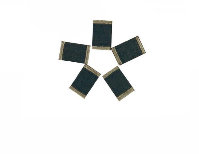
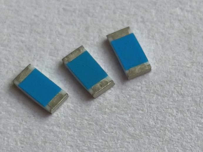
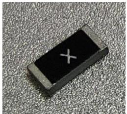
部分陶瓷天线实物图